The role of DUV coatings in enabling the next generation of semiconductor devices
Between the global shortage of microchips, the ravenous demands for ever greater computing power and the mind-blowing complexity of the modern-day integrated circuit (IC) manufacturing process, the semiconductor industry is on a constant look out for creative solutions.
Where precision counts, as it most certainly does in the world’s multi-billion-dollar semiconductor fabrication facilities, each and every part of the system must perform – there can be no weak links. This is true down to the choice of optical coatings utilized by semiconductor equipment manufacturers. In fact, leveraging the latest innovation in optical coatings technology is helping to meet the evolving requirements of today’s semiconductor industry.

Shorter wavelengths for higher quality inspection
Defect detection is one area, in particular, where optical coatings are an important enabler. Effective inspection not only improves yields and throughputs, it ensures chip reliability. For safety-critical applications, such as defence technology or autonomous vehicles, avoiding in-field failures is paramount. But finding defects is becoming increasingly challenging due to the smaller and smaller feature sizes of modern-day semiconductor devices.
Within the array of tools deployed as part of the back-end semiconductor inspection process, optical coatings play a significant role in facilitating the shorter wavelengths required to spot the smallest defects on the tiniest chip. For decades, the reduction in size and exponential increase in transistor density has (broadly) followed Moore’s Law. This has seen the number of transistors squeezed onto a chip double every two years. But with miniaturization down to the sub-5 nm scale, inspection becomes incredibly challenging; the only way it can be achieved is with shorter wavelength UV light and higher fluences than used previously.
Semiconductor inspection tools measure light that is scattered by defects and imperfections. Shorter wavelength lasers at higher fluences improve the sensitivity as more light is scattered and therefore smaller defects and imperfections can be spotted. Since DUV coatings with high transmission and low loss increase the fluence at the desired lower wavelengths, tool manufacturers can more easily achieve the necessary level of resolution and sensitivity to ‘see’ defects just a few nanometres in size. In fact, a tool optimized at 213 nm can detect an anomaly as small as 5 nm.
Maintaining momentum on DUV innovation
As demand continues to outstrip supply in the continuing grip of a global chip shortage, no one can afford to take their foot off the pedal in EUV and DUV development. Against this backdrop, G&H is bringing its renown pedigree in UV technologies to bear to optimize laser tool performance at shorter wavelengths, overcoming the limitations of current tools.
The latest development is an anti-reflection coating at 213 nm on quartz. This durable oxide coating has excellent environmental performance and its deposition is optimized to control absorption at the target wavelength.
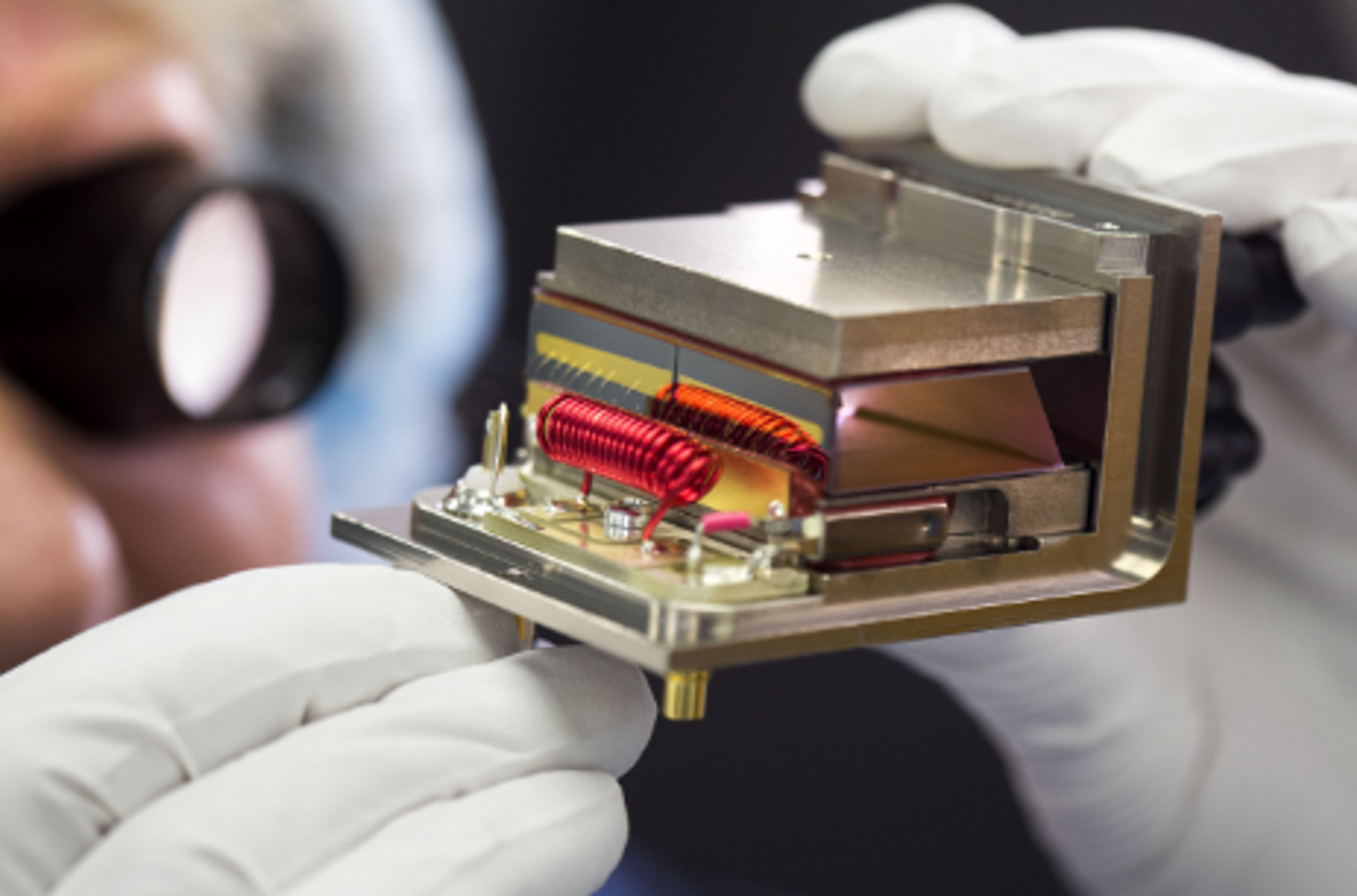
These DUV coatings can be applied to a myriad of G&H optical components used in semiconductor processing, including waveplates, acousto-optic deflectors and modulators. Inspection tools that incorporate our low loss DUV coated optics and acousto-optic devices, provide for higher fluence at shorter wavelengths, thus improving sensitivity for reliable defect detection, even with lower power lasers.

“Adding value throughout the chain”
However, the true potential of this latest development lies in our track record in DUV technologies across the board. The quartz substrate, for example, is prepared and polished in-house and married to the coating in the same Class 5 cleanroom to ensure chemical stability. The coating is made from durable oxide that resists scratching and degradation, optimized to control absorption and maximise sensitivity. G&H is also the world's leading supplier of UV acousto-optic deflectors and modulators, and the only entirely vertically-integrated CdS, CdSe, KDP and KD*P waveplate producer, with the added strength of being able to mount waveplates to custom specifications.
“Our strength is drawing on the great capability across the G&H group to offer an all-in-one solution,” explained Peter Williams, Head of UK Precision Optics and Systems at G&H. “Our end-to-end offering across DUV technologies is a unique combination, underpinned by the expertise of our world-leading scientists and engineers. This enables us to control each stage of the process, adding value throughout the chain. For our customers, this level of control means high-tech, optimum efficiency solutions at much lower risk.”
How low can you go?
The 213 nm coating is not the end game as G&H applies our high-tech, low risk model to push further. “All roads lead to shorter wavelengths to keep pace with miniaturization,” Williams said. “We are strong enough with the broadest capability to make a real difference on DUV coatings to enable better performance, greater reliability and higher efficiency. Building on our pedigree in coatings technologies, it’s an exciting journey of discovery that will ultimately unlock further benefits for semiconductor equipment manufacturers.”
Industrial and telecom solutions
G&H designs and manufactures submodules and module assemblies according to customer specifications.