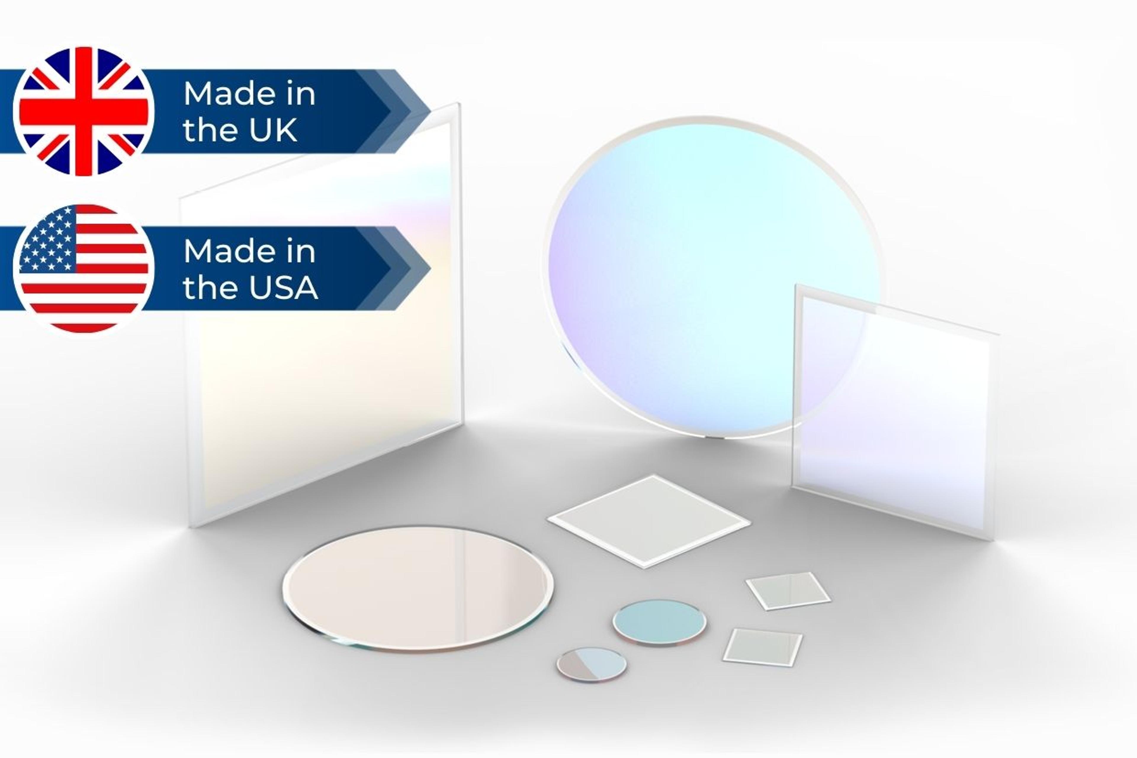


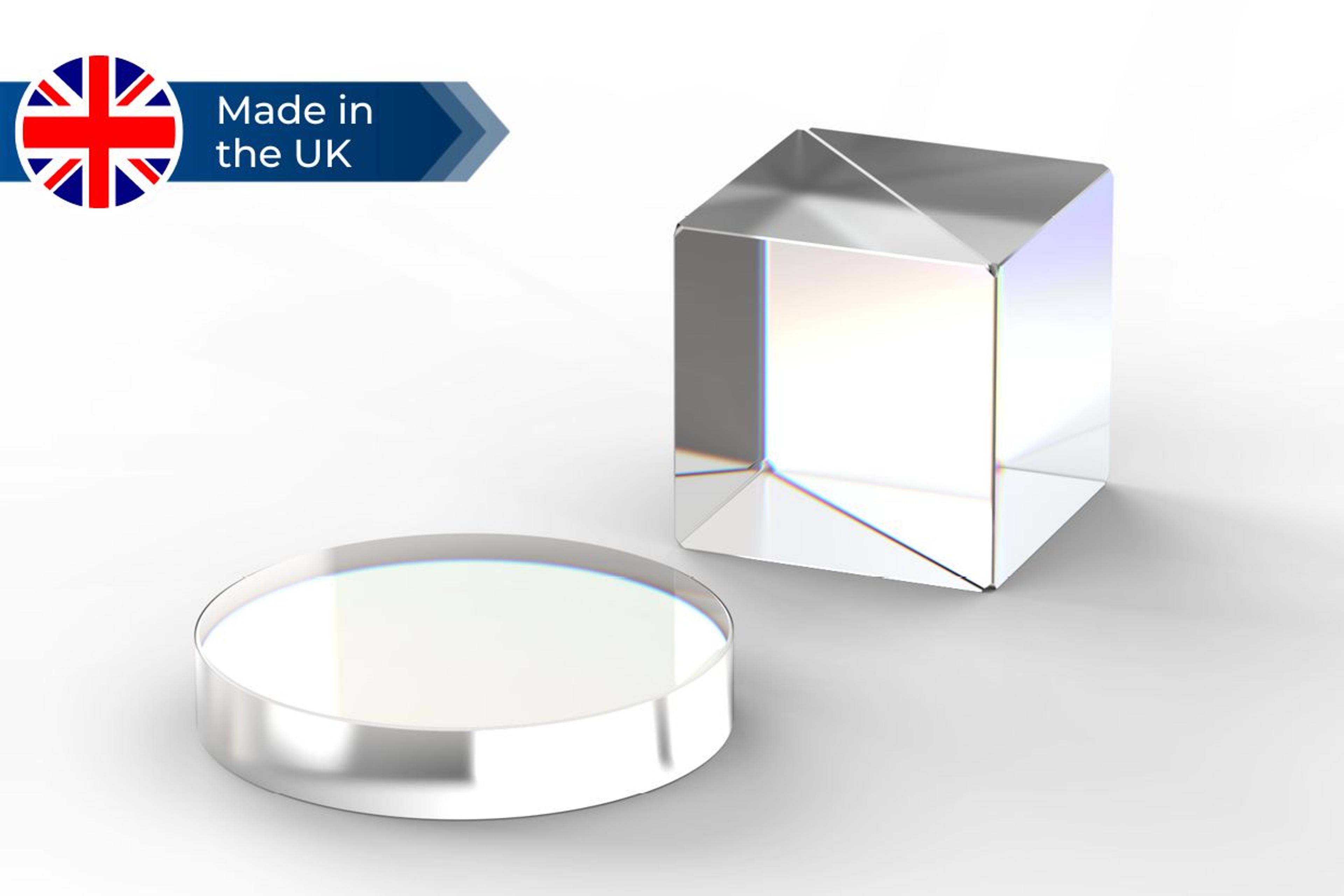
Beamsplitters
Plate and cube beamsplitters that have superior laser damage performance for each unique wavelength, split, and incident angle combination
Find out more
Laser processing is driving a revolution in semiconductor manufacturing, enabling smaller, thinner technology. Our OEM laser solutions support industrial innovation and efficiency.
Semiconductors are a key enabler for many technologies. As devices become more compact, the footprint of components gets smaller. To keep pace, laser technology is using ever shorter wavelength sources.
As experts in the optical development of semiconductor processing, we are innovating in laser based technologies to bring benefits to manufacturing applications, including laser cutting, drilling, marking and measuring.
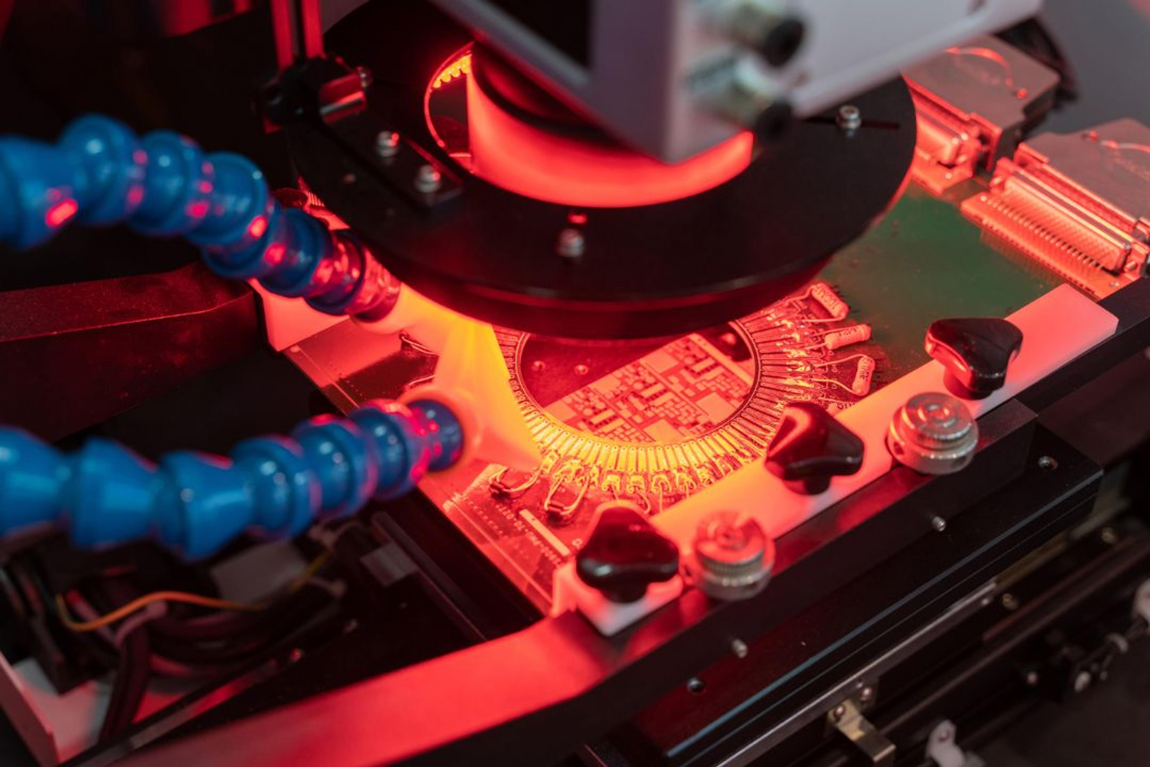
In order to reliably and effectively process semiconductors, accurate control of the laser beam is a necessity. Our acousto-optic deflectors enable this extreme level of control. We grow our own high quality optical crystals to give us complete control over the material, and in combination with our finishing capabilities, this results in the highest quality acousto-optic devices on the market.
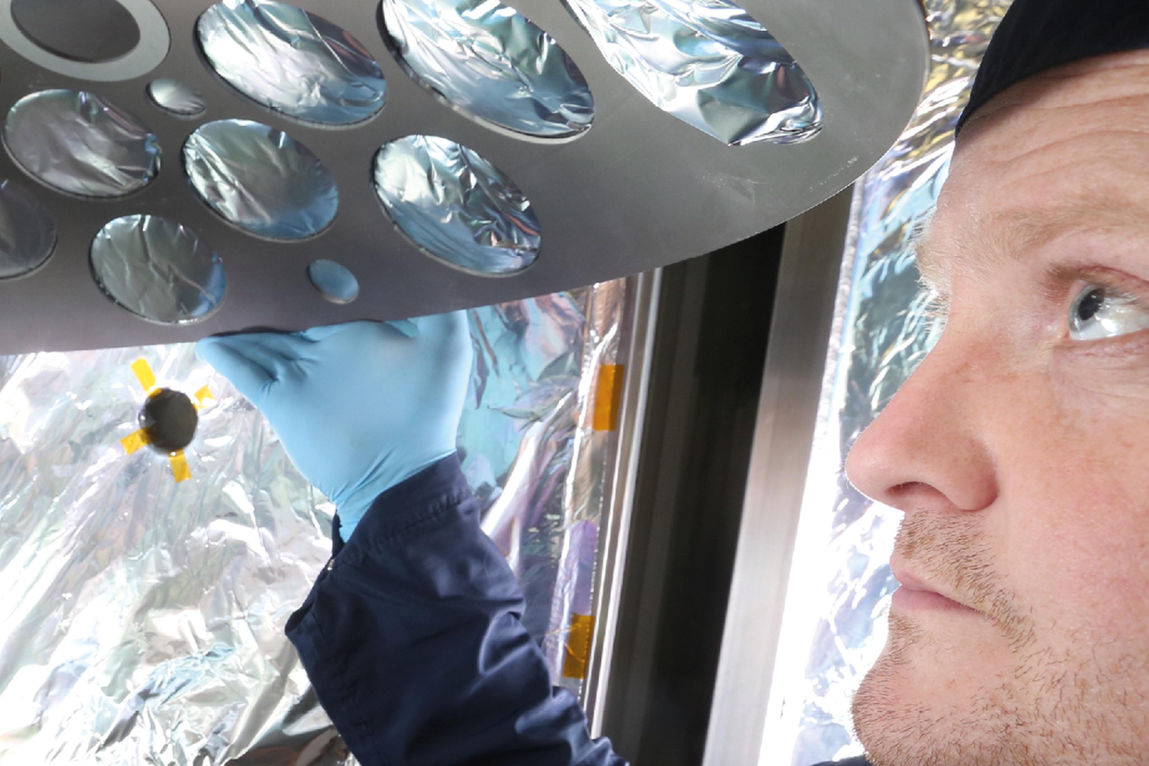
Our specialist optical coating is optimized for the key wavelengths of DUV semiconductor manufacturing at 193 and 213 nm. Coating optical materials requires a clean environment to avoid contamination, which greatly reduces the power handling and longevity of the coating. Our expertise in coating has been supported by investment in custom built, ultra-clean, high repeatability chambers to meet the evolving demands for environmentally-stable optical coatings.
UV is generated by focusing lasers onto a target to create plasma. Incredibly high powers and short durations are required for this process, and there are several challenges to get down to such short wavelengths. The goal is high quality, fast processing which requires optical power stability, beam position accuracy and stability, and short laser pulse duration. Our germanium acousto-optical modulators (Ge AOMs) provide solutions to these challenges by enabling power stabilization, precise and stable beam positioning, and pulse duration control below 1 us.
In semiconductor and microelectronic processing, metrology is the measurement of perfection. Very specialized metrology and manufacturing in this field requires extreme precision in imaging and aberration control. When features are nm in size, small errors can result in millions of lost investment. In addition, components must remain precise and long-lasting in harsh UV environments.
Shipping fully-compliant products requires close management and control of the complete manufacturing value chain, including operator training, independent quality auditing, in-process testing, cutting-edge equipment, meticulous process design and management. And, of course, everything is underpinned by a specialist, compliant environment in which the manufacture takes place.
The key to a successful finish is packaging. G&H has rigorous standards that exceed compliance norms. The vacuum packaging used for all our components and assemblies is nitrogen-flushed, to ensure the packaging itself does not become a source of contamination. This means we can be as confident of our standards at the end of the process as we can at the beginning and throughout.
Working across DUV and UV, we offer a wide range of products and services to underpin the latest manufacturing techniques and innovations in semiconductor processing and devices, including:
• Acousto-optic deflectors for DUV (193/213 nm) processing
• Ge acousto-optic modulators for UV (13.5 nm) sources
• Multi-channel modulators
• Beam control and imaging optics
• Inspection optics for UV, zoom or fixed magnification
• Waveplates
• Custom optical coatings from 193/213 nm
• Coated substrates also available
We also offer optomechanical and electronic design, including finite element analysis (FEA).