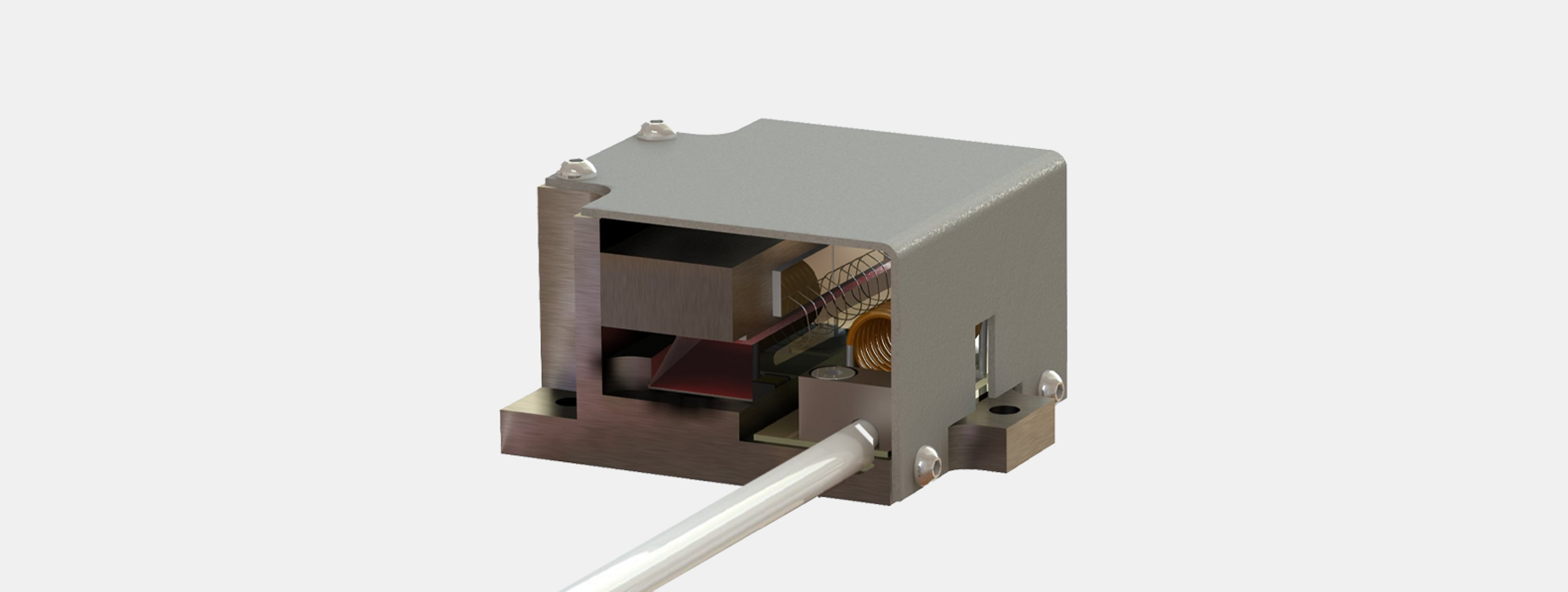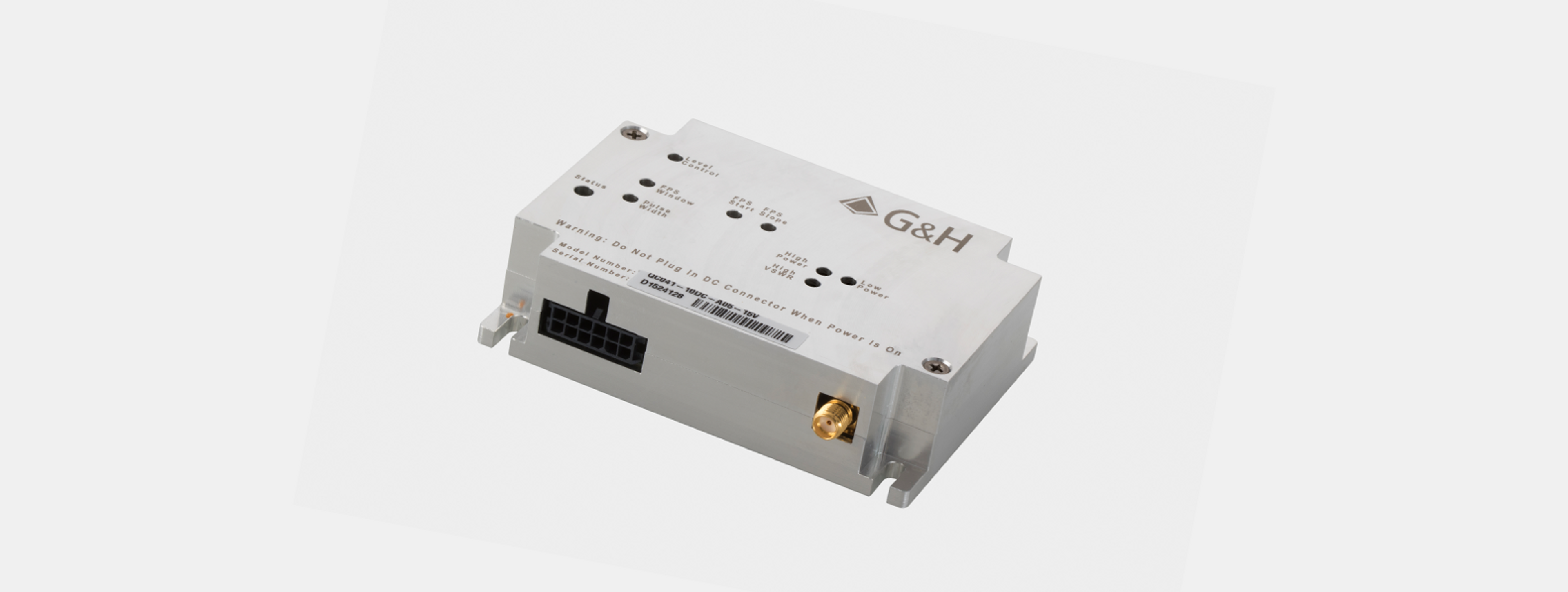
Compact Low Power RF AOM and AOQS Driver
With an operating frequency of 24–110 MHz, a 24 W output into a 50-ohm load, and analog and digital modulation.
Full Product Description- RF output power:
- 2 to 24 W
- RF frequency:
- 24.00 MHz, 27.12 MHz, 40.68 MHz, 68.00 MHz, 80.00 MHz or 110.00 MHz
Product description
A compact low-power RF driver designed to drive acousto-optic modulators and q-switches, with two digital modulation inputs with a fixed designated width or variable width corresponding to the input signal's pulse width.
This driver has a zero crossing function where the output pulse can be synchronized to the zero crossing point of the RF Energy. When enabled the pulse to pulse stability is improved.
Key features
- 24, 27.12, 40.68, 68, 80, or 110 MHz RF frequency (XXX)
- 0.01% quartz stabilized
- Up to 24 W RF power output (YY)
- Two TTL digital modulation inputs: fixed and variable pulse width
- Up to 1 MHz pulse rate in Q-switch applications.
- Up to 10 MHz pulse rate in pulse picking applications
- Analog modulation or triggered RF Ramp Down Mode (ZZZ)
- Synchronization to RF by ‘zero cross’
Specifications
| Name | Value |
|---|---|
| Supply voltage | +12, +15 or +24 VDC (factory set) |
| Supply current | ≤ 3 A |
| RF output power | 2 to 24 W |
| Output impedance | 50 Ω |
| RF frequency | 24.00 MHz, 27.12 MHz, 40.68 MHz, 68.00 MHz, 80.00 MHz or 110.00 MHz |
| Frequency stability | ± 0.01% |
| Extinction ratio | ≥ 50 dB |
| Harmonic distortion | ≤ -20 dB for units with output power ≤ 15 W, ≤ -15 dB for units with output power > 15 W |
| Spurious levels | ≤ -50 dBc |
| Analogue modulation impedance | 1.5 k Ω |
| Analogue modulation voltage range | 0 to +5 VDC ¹ |
| Digital modulation impedance | High impedance |
| Digital modulation level | TTL compatible (V_IL < 0.8V, V_IH > 2.0 V) |
| Mod in fixed | Standard: Triggered on rising edge, Inverted digital input option (NEG): Triggered on falling edge |
| Mod in variable | Standard: TTL V_IH = RF OFF, Inverted digital input option (NEG): TTL V_IL = RF OFF |
| FPS/PPK input impedance | High impedance |
| FPS/PPK input level | TTL compatible (V_IL < 0.8V, V_IH > 2.0 V) |
| Trigger | Standard: Triggered on rising edge, Inverted digital input option (NEG): Triggered on falling edge |
| Rise/fall time | Digital/analogue modulation: ≤ 35 ns (10 to 90% RF power) ² |
| Zero crossing enable input impedance | High impedance |
| Zero crossing enable input level | TTL compatible (V_IL < 0.8V, V_IH > 2.0 V) |
| Trigger | Standard: TTL V_IH or no connection - disabled, TTL V_IL - enabled, Active zero cross option (ZC): TTL V_IH or no connection - enabled, TTL V_IL - disabled ³ |
| Sync output | 3.3 V signal, inverted in ZC units |
| Enable input | < 3 W dissipation in standby mode |
| Normal operation | TTL V_IH or no connection |
| Standby mode | TTL V_IL |
| Driver reset | Momentary TTL V_IL |
| Operating temperature | +10 to +55°C case temperature, non-condensing |
| Storage temperature | -20 to +85°C, non-condensing |
¹ The voltage range corresponds to 0 to 100% of the pre-adjusted maximum RF output power. For units configured with A05, R05 and M05.
² into 50 Ω load
³ ZC option enables zero cross by default
Output Indicators
| Status indicator LED | |
|---|---|
| Red | Normal operation |
| Green | Standby mode |
| Yellow | Fault condition |
Connectors and Mechanical Data
| RF output connector | SMA Female (recommended torque 0.45 Nm max 0.6 Nm). |
| Power and control connector | Molex 0430451221 |
| Mating connector | Molex 0430251200 with Molex 0430300008 crimp terminals |
| Cooling method | Contact cooled |
| Cooling spec | The driver must be attached to a heatsink capable of dissipating; |
| 36W @ 12 V | |
| 45W @ 15 V | |
| 72W @ 24 V | |
| Weight (driver only) | 192 grams |
Connector Pinout
Power and control connector
12 positions header connector 0.118" (3.00mm)
All input signals refer to ground (GND) unless otherwise stated. All outputs are open collector type 25 mA max current drain.
| Pin assignment | |||
|---|---|---|---|
| Pin 1 | SYNC (out) | Pin 2 | FPS trigger (in) |
| Pin 3 | Mod in fixed (in) | Pin 4 | GND |
| Pin 5 | Mod in variable (in) | Pin 6 | Mod in analog (in) |
| Pin 7 | Zero cross enable (in) | Pin 8 | Low power fault (out) |
| Pin 9 | High power fault (out) | Pin 10 | High VSWR load fault (out) |
| Pin 11 | Enable (in) | Pin 12 | VDC |
Absolute Maximum Ratings
Important: Failure to remain within stated rating may cause instantaneous and irreparable damage to the driver.
| Supply voltage | +27 VDC | |
| RF power output | No DC feedback allowed | |
| TTL/analog signal inputs | -0.5 V to +5.5 V | |
| Mod in fixed minimum pulse width | 50 ns | |
| Modulation repetition rates | Mod in fixed | 1 Hz to 1 MHz |
| Mod in variable | DC to 10 MHz |
RF Power (W) Frequency (MHz)
| Supply voltage | 24.00 MHz | 27.12 MHz | 40.68 MHz | 68.00 MHz | 80.00 MHz | 110.00 MHz |
|---|---|---|---|---|---|---|
| 12 V | 10 W | 10 W | 10 W | 10 W | 10 W | 10 W |
| 15 V | 24 W | 24 W | 24 W | 20 W | 20 W | 10 W |
| 24 V | 24 W | 24 W | 24 W | 24 W | 24 W | 10 W |
Adjustments
| RF Power Level Adjustment | Adjusts the output RF Power – clockwise increases power output |
| LP – Low Power Set Point | Adjusts the minimum power threshold. The LP Fault output goes LOW if the output power is below this level ⁴ |
| HP – High Power Set Point | Adjusts the maximum power threshold. The HP Fault output goes LOW if the output power is greater than this level. |
| High VSWR Set Point (HVSWR) | Adjusts the module’s tolerance for a mismatched load connected to RF Out. If a mismatch is detected, the HVSWR Fault output goes LOW, the status LED will change to YELLOW, and the driver will cease output until reset by momentarily entering standby mode. |
| Pulse width (Mod in fixed) | Adjusts the length of time the driver outputs no RF energy after receiving a Fixed Input trigger. 1 µs to 20 µs. |
The following adjustments are used on units configured with FPS or PPK:
| FPS Start | Adjusts the initial power level of the first pulse. |
| FPS Slope | Adjusts how quickly the RF pulses return to their normal level after the FPS has been triggered. 20 µs to 300 µs. |
| FPS Window | Adjusts the duration of the suppression pulse cycle. 20 µs to 300 µs. |
⁴ The LP Fault output will be suppressed whist modulating the RF power via analog modulation.
Order code
XXX = 024, 027, 041, 068, 080, or 110 as standard where RF Frequency = 24.00, 27.12, 40.68, 68.00, 80.00 or 110.00 MHz.