Germanium Wafers
High-purity Germanium wafers engineered for infrared detection, semiconductor fabrication, and photonic applications in sensing, imaging, and optoelectronic systems.
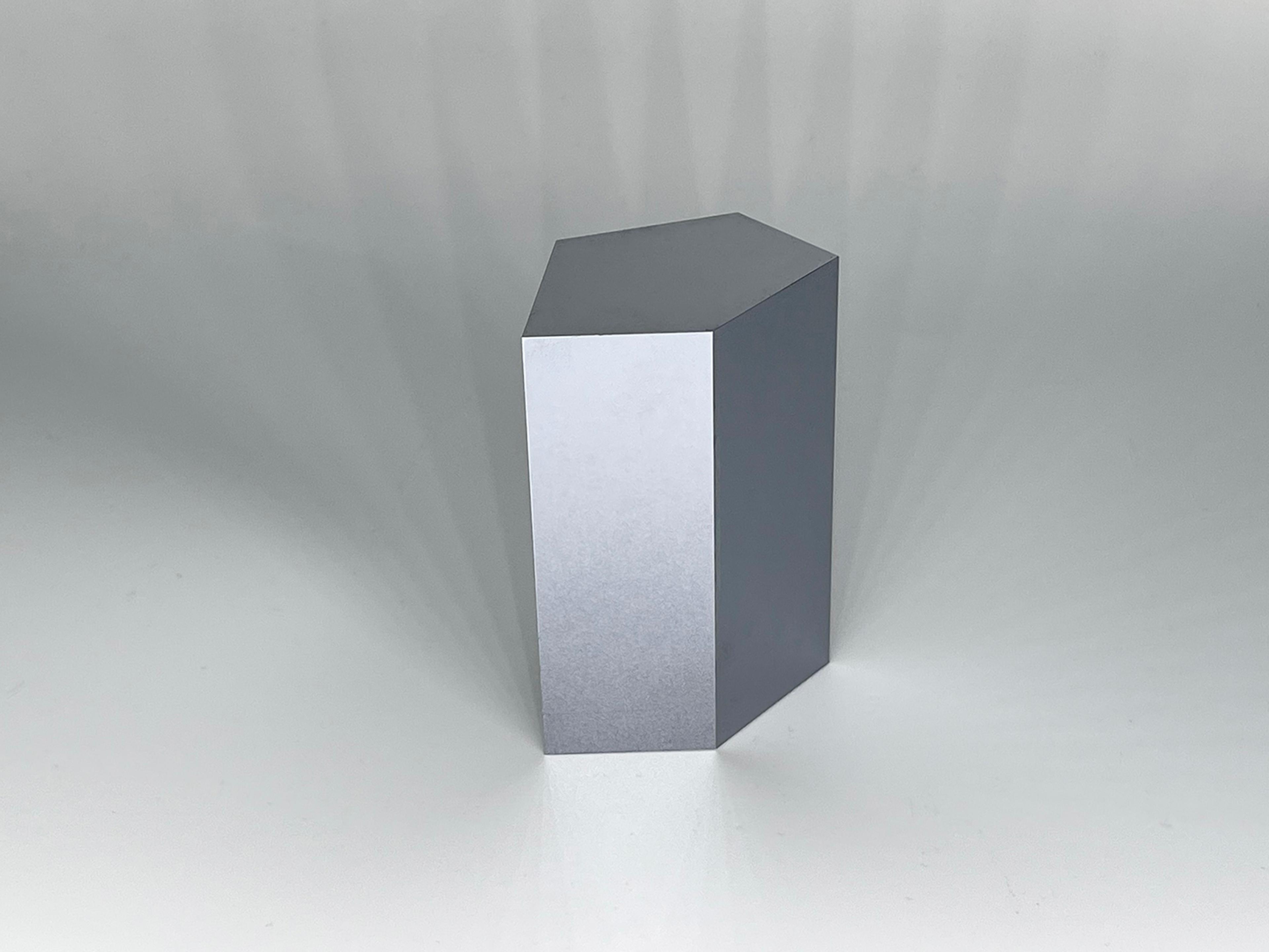
Full Product DescriptionProduct description
G&H Germanium wafers are precision-manufactured from high-purity monocrystalline Germanium for use in infrared (IR) detection, semiconductor devices, and advanced photonic systems. These wafers offer excellent transmission in the mid- to long-wave infrared range (2–14 µm), making them ideal for IR detectors, thermophotovoltaic cells, and spectroscopic sensing.
Available in both intrinsic and doped forms (n-type or p-type), G&H Germanium wafers feature low dislocation density, excellent surface quality, and tight dimensional tolerances. They can be supplied in standard semiconductor-grade diameters with polished, lapped, or etched surfaces depending on downstream processing requirements.
With applications in aerospace, defense, medical diagnostics, and industrial sensing, Germanium wafers support high-sensitivity devices operating across a wide range of infrared wavelengths.
Key features
- Excellent IR Transmission: High transparency from 2–14 µm for IR detectors and sensors
- Doping Options: Available as intrinsic, n-type (phosphorus), or p-type (gallium/boron)
- High Purity & Crystal Quality: Low dislocation density for semiconductor-grade performance
- Custom Surface Finishes: Supplied lapped, etched, or double-side polished
- Standard Wafer Sizes: 2", 3", 4", 6", and 8" diameter options
- Electrical & Optical Tunability: Tailored for optoelectronic and photonic device needs
- Thermal and Mechanical Stability: Excellent dimensional stability and processing compatibility
- RoHS and REACH Compliant
Applications
- IR detectors (MWIR and LWIR photodiodes)
- Thermophotovoltaic (TPV) energy systems
- Semiconductor fabrication (transistors, solar cells)
- X-ray and gamma-ray detectors
- Biomedical sensing and diagnostics
- Environmental and gas analysis systems
- Infrared spectroscopy and photonics research